Monthly Archives: May 2013

Why The Nanoscale Matters

One of the most intriguing experiences in science is observing something  completely counterintuitive. And then having to figure out, okay, why is everything I thought I knew wrong in this case, and what experimental or theoretical studies can I do that will help explain this? That’s the appeal and the challenge of nanoscience: things at a small scale behave very differently from what we’d guess based on observations at a large scale. So how does weirdness inherent in the quantum world come into play?

A single atom has different properties than a bulk material that has trillions of atoms together. That’s because there are a discrete number of possible configurations for the atom to be in, which means discrete energy levels. This is called quantization, as opposed to the continuous smear of available configurations and energy levels that a bulk material has. But if we move away from the extreme cases, where does bulk behavior stop and quantized behavior kick in? Are two atoms still a quantum object? Three? It turns out that quantization of material properties actually persists for awhile, and collections of hundreds or thousands of atoms can still show quantization.

So how do we know where the transition point is between bulk and quantized properties? If we think about shrinking a material down, at some point the size of the material will become smaller than the size of the electronic wavefunction in that bulk material. Below that size, the electrons are “confined” and the states available to them start to change depending on the material size. So we can define a length that is a “quantum confinement limit” for each material. Below the limit, the collection of atoms is confined and has quantum properties, and above the limit it’s approximately the same as a bulk material.

Once we know that limit, there are several ways to make nanomaterials that have quantized properties. We can make nanostructures that are confined in one dimension, like nanosheets, but bulk-like in the other two. We can also make nanowires, which are confined in two dimensions but have one bulk-like dimension. Or, we can make “quantum dots” which are confined in all three dimensions. Quantum dots are like little islands of material, with discrete energy levels just like an atom would have. And one consequence of quantization is that the wavelength of light that quantum dots absorb and emit actually depends on size, as in the image below. Smaller quantum dots absorb and emit bluer light, because the size of the quantum dot increases the spacing between energy levels. There are lots of applications for this effect, such as solar cells whose absorption spectrum is tuned to that of the sun, or LEDs that emit tunably-colored light.

But at the nanoscale, the surface of the object is a lot more important. In something macroscale, like a brick,  less than 0.0001% of the atoms are on the surface of the object, but in a quantum dot 30% of the atoms may be surface atoms. That makes surfaces very important! And surface atoms can be the sites of electronic defects, or the sites of bonding by various chemical species that change the properties of the quantum dot. So surface chemistry becomes important, and the quantum dot or nanowire or nanosheet may be very sensitive to small changes in the environment. This can be an asset, though, for example to make gas sensors from chemically functionalized nanomaterials.

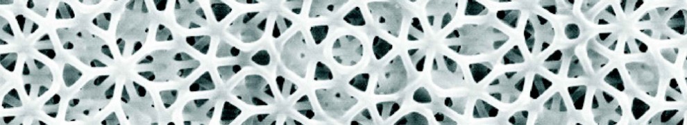
Another consideration is that if a material has some features that are nanoscale, those features may be as small as or even smaller than the wavelength of visible light. Practically speaking, this means it’s often easier to image nano-objects with electrons rather than photons. But again, there’s an upside, because you can tune the nanoscale features to interact with light in specific ways or even be hidden from interactions light. This is one of the most interesting things about metamaterials, which I’ll write more about soon!

Defects in the Crystal Structure of Materials

Describing phenomena from the real world mathematically has a tempting sort of elegance and simplicity, but there’s a danger of oversimplifying. You risk missing out on some of the really complex beauty that’s out there! I always experience a bit of glee when a simple explanation turns out to miss something messy but important, and for that reason I’d like to tell you about defects in crystal structure and why they matter.

Awhile back, we talked about periodic structure in solids, and how the geometric arrangement of atoms in a material determines many of the material properties. For electronics, the density of mobile charge carriers (electrons or holes) and the availability of energy states for those carriers to occupy are the two main relevant material properties. From these we can get metals, which conduct electrons easily, or insulators, which don’t, or semiconductors which are somewhere in between. Modern computing is largely based on devices built from semiconductors, connected to each other using metals, with insulators used for electrical isolation and a few other tricks.

But while it’s helpful to imagine a perfect material, with each atom positioned just where it should be in an infinitely repeating array, nature is messy. We can learn a lot from theoretical material models, but the materials we find in the real world will be different. We call any deviation from perfect crystal lattice structure a defect, and the interesting thing about defects is that they can affect material properties too, especially with nanoscale objects that can have a high ratio of “defect” atoms to “normal” atoms.

There are a few different kinds of defects one finds in natural materials. For example, an atom might be missing from a lattice site which is called a vacancy, or there might be an extra atom where there shouldn’t be which is called an interstitial. There could be a whole plane of atoms that just starts in the middle of the crystal, which is called an edge dislocation. Or two regions with different orientations of their crystal structure might be pressed up against each other, which is called a grain boundary. There are lots of ways that a crystal lattice can get messed up, but remember, for that material, the native crystal lattice is usually the minimal energy solution for packing a bunch of atoms together with those properties. So the most probable outcome for any given region is a perfect lattice, but the material will end up with some deviations from this as well. How many defects there are depends on how energetically favourable the lattice is, but also on how the material was made: if you solidify a crystal really slowly, the atoms are more likely to find the true lowest energy position (sites in the perfect lattice) and there are fewer defects.

These defects all matter because they affect material properties, so if we assume that a material is going to behave as it would with a perfect crystal lattice, we are in for a surprise! If we’re focused on practicalities, like whether the material is as electrically conductive as we think it should be, then the type and concentration of defects in the device is very important, because some defects will reduce current flow and others will enhance it. To understand why, let’s think about the physical mechanisms for current flow through a material.

In a crystal, we have an array of positive nuclei with some tightly bound electrons that are bound to them; we can call these ‘localized’ electrons because they are staying in the same approximate location around the nucleus. Electrons that were more loosely bound to the original atoms are able to move freely through the crystal; when these ‘delocalized’ electrons move through the material, that is what we can measure as current flow. But a large part of the reason we can even have delocalized electrons is due to the periodicity of the lattice, which mathematically allows delocalized wave states for the electrons. When this periodicity is broken, as it is by dislocations and grain boundaries, the wave states can be disrupted, and new bound states that localize electrons to the defect are created. These are often called ‘charge traps’ because they trap the charge carriers in a specific place. However, if we ‘dope’ a material by carefully adding lots of interstitial atoms that have an extra electron, we can avoid disrupting the wave states for electrons, but add more electrons total, which actually increases the conductivity of the material. So in device manufacture, controlled doping is a common use of defects to affect material property, but dislocations and grain boundaries are often avoided because their effect on the material property is usually undesirable.

In nanoscience defects are even more important, because with a nanoscale object that’s just hundreds of atoms across instead of hundreds of billions, the percentage of atoms that are in non-ideal crystal sites can get pretty high. For example, many surface atoms end up as defects that trap charge, and a nanocrystal may be 30% surface atoms! So lots of nanoelectronics research is focused on minimizing the negative impact of defects. However, there’s an interesting contradiction there: the fascinating thing about nanomaterials is their quantum-like properties compared to bulk materials. But quantization  in nanomaterials stems largely from the greatly increased number of grain boundaries and surface atoms and defects, because these things all increase as you scale down the size of the material. So there’s a careful balance between mitigating the negative effects of defects, and not getting rid of the nanoscale-specific behaviors that make nanoelectronics interesting in the first place!